


The Best Time to Visit Spain
The second largest country in Europe, Spain has incredibly diverse landscapes, from golden beaches along the coast to dramatic mountain ranges. It’s also home to world-class art and museums, incredible historic sites, medieval hilltop villages and cosmopolitan cities. In order to determine the best time to visit Spain, it really depends on the destinations you plan to visit and what you’d like to do.
In many areas of Spain, the Mediterranean climate makes spring and fall the best times to visit, with mild weather for enjoying the sights, whilst those who want to ski its famous slopes will want to come during the winter. This overview will provide a more in-depth look to help you decide when to go for the best possible experience.
Speak to the Expert
With its rich cultural heritage, the best time to visit the historical cities and sites of Andalucia is during the spring and fall, as the region’s intense summer heat makes it unpleasant for sightseeing during this time.
Ally
European Specialist


Mid-March - May
Spring
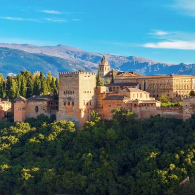
Spring is an ideal time to visit Spain – in most places the weather will be quite pleasant, although mountainous destinations in the north may be a bit chilly. This is the best time to visit cities inland like Seville, Cordoba, Madrid and Grenada, with things warming up but not becoming unbearably hot. In the capital city, the average daytime temperatures now tend to hover in the upper 60s to low 70s Fahrenheit. At Alhambra Palace, a must-visit, you’ll be able to miss the thickest tourist crowds while enjoying the sights. The beaches are likely to be warm enough to relax on although the water may be a bit too cool for swimming.
see more...
June - August
Summer
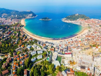
Summer in Spain is very warm and crowded. In southern destinations, including cities like Cordoba, Malaga and Seville, it can become unbearably hot. Even in the capital city, the mercury often rises to 99 degrees or above, and in Barcelona it will be humid but not as hot. This is the best time to visit northern locations, including San Sebastian on the Atlantic coast, and enjoy hikes in the mountains like the spectacular Pico de Europa. This is also the time the beaches will be at their best for swimming, although most stretches will be jam-packed. It’s the busiest time of the year, which means you’ll need to book your accommodation while in advance, and plan for tourist crowds.
see more...
September - November
Fall
The fall is one of the best times to visit Spain, with the summer heat dissipating and the crowds beginning to diminish. Airfares are often lower around this time and accommodation rates discounted following the peak of the tourist season. The weather is likely to be mild and pleasant in many areas, particularly in central and southern Spain, although it will be cooler in the north. The later in the season you come, the more those temperatures will drop. In Madrid, averages range from a high of 89 degrees during September to mid-60s in October and the mid-50s in November. The Pyrenees Mountains are likely to start seeing snow by the later part of the season. If you visit the world-renowned La Rioja wine region in northern Spain, you can enjoy the Rioja Wine Festival which celebrates the season’s first harvest around the third weekend of September, with grapes pressed by men wearing traditional clothing in a large wooden tub, food tastings, bullfighting and more.

December - Mid-March
Winter
Winter is the low season, with even the beaches in the south of Spain too chilly for sunbathing. Central Spain is typically the warmest with Madrid seeing high temperatures in the mid-50s to low 60s. It’s the time to come for skiing, with lots of snowfall in the north, particularly in the Pyrenees. There will be Christmas Markets throughout the country in December, with Barcelona offering one of the best.
Luxury Spain Private Tours
-
Explore This Trip
Highlights of Spain
Madrid, Seville, Granada, Barcelona
10 NightsFrom £3,760 PPAn unforgettable adventure through Spain’s most popular cities with connections by high-speed... -
Explore This Trip

Spain: Cities & the Sea
Barcelona, Madrid, Mallorca
9 NightsFrom £3,345 PPIf you’re looking for a mix of exciting cities with lively energy and a place to relax with beautiful... -
Explore This Trip

Idyllic Andalucia & Catalunya
Seville, Granada, Barcelona, Costa Brava
12 NightsFrom £4,590 PPWithin the borders of just one country, there’s lots to see, and this 13-day, 12-night trip allows...
Ready to plan your trip?
What ever you want from your dream trip, our team of
experts are ready to help.
You may be interested in
-
The 10 Best Things to Do in San Sebastian, Spain
The city of San Sebastian in Spain, known officially as Donostia, is located in the Basque region in the north of the country. Home to…
-

8 Best Things to Do in Barcelona in 3 Days
The Mediterranean bliss that is Barcelona, nestled on the northeastern coastline of sunny Spain, is one of the country’s most lively and thriving destinations. Its…
-

10 Best Things to Do in Seville in 2 Days
As the fourth largest city in Spain, Seville offers much to mesmerize and fascinate those who visit its architecturally impressive sights and venture through its…
COPYRIGHT © 2024 UNFORGETTABLE TRAVEL. ALL RIGHTS RESERVED